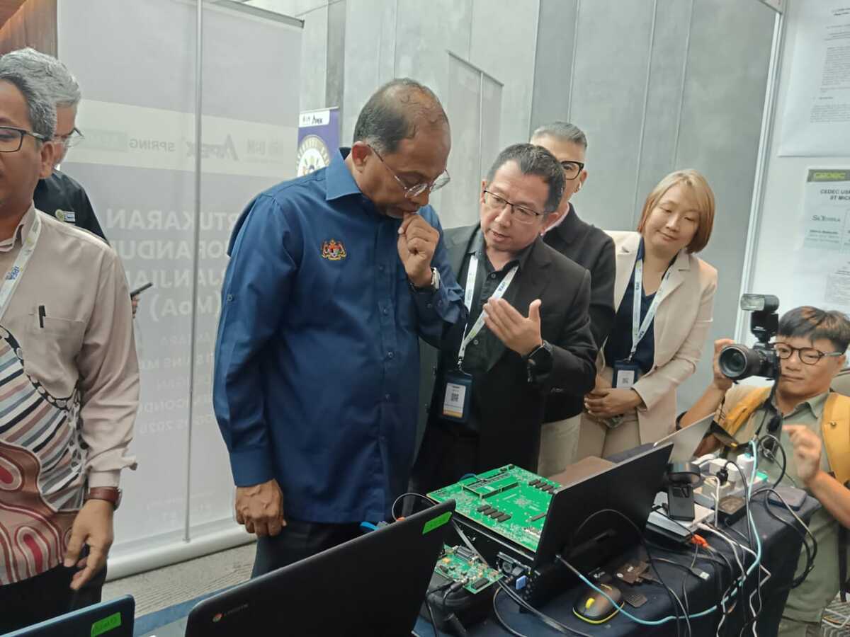
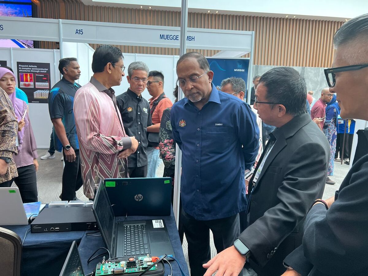
Malaysia’s aspiration to become a regional semiconductor powerhouse hinges on more than factories and funding—it demands mastery of chip design. To achieve this, Spring Semiconductor (SpringSemi) and CEDEC Malaysia have co-developed SpringBlade, the nation’s first SoC prototyping platform, tailored for education, research, and industry acceleration.
SpringBlade is a strategic milestone aligned with the National Semiconductor Strategy (NSS), designed to empower Malaysia’s IC designers, train the next generation of engineers, and prototype world-class silicon systems—from RTL to TSMC tapeout—right here at home.
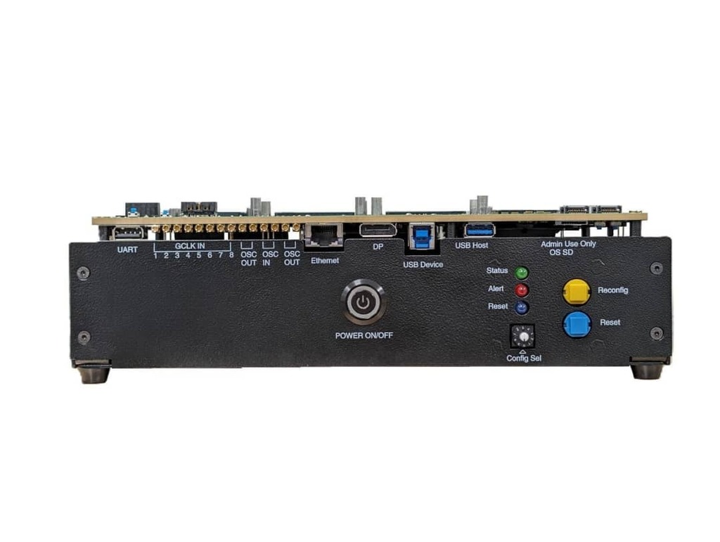
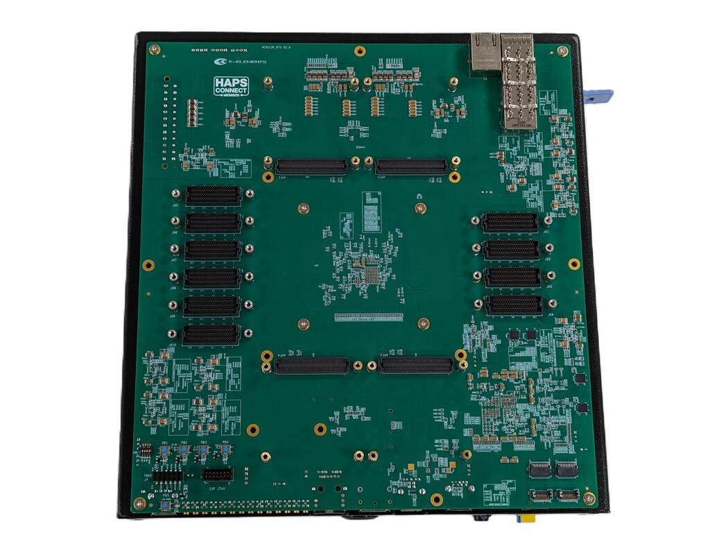
SpringBlade+ is the first platform in the SpringBlade family.
Built on the Xilinx VU13P FPGA architecture, it combines:
The platform was designed to support:
SpringBlade includes integrated remote-access infrastructure through its HaaS model.
This enables engineering teams to:
Supported capabilities include:
This model allows organizations to access advanced prototyping infrastructure without maintaining large in-house FPGA labs.
Each Springblade system is compatible with a library of over 50 development modules:
All modules are hot-pluggable, reconfigurable, and supported by a unified SDK.
SpringBlade is a family of FPGA-based prototyping and hardware acceleration platforms developed by Spring Semiconductor to support ASIC validation, SoC development, software bring-up, and advanced hardware experimentation.
Built for engineering teams, universities, startups, and ecosystem builders, SpringBlade enables practical semiconductor development without requiring the massive infrastructure costs associated with traditional emulation systems.
Modern semiconductor development has become increasingly difficult due to:
Many organizations cannot justify the cost of large-scale emulation systems from providers like Synopsys or Cadence Design Systems.
SpringBlade was created to provide a more practical and economically accessible path for:
especially within the ASEAN semiconductor ecosystem.
FPGA-based prototyping uses programmable hardware platforms to validate and execute ASIC or SoC designs before manufacturing.
Compared to simulation alone, FPGA prototyping enables:
Compared to full emulation systems, FPGA prototyping offers:
This makes FPGA-based prototyping one of the most practical approaches for many semiconductor teams.
SpringBlade systems are designed around scalable FPGA architectures optimized for:
The platform supports:
Spring Semiconductor is expanding the SpringBlade platform toward larger-scale adaptive computing and high-density prototyping systems.
Upcoming systems include:
These next-generation platforms target:
| Area | Application |
|---|---|
| ASIC Prototyping | Pre-silicon validation |
| SoC Validation | Hardware-software integration |
| AI Systems | Hardware acceleration and experimentation |
| Embedded Systems | Firmware and driver bring-up |
| Universities | Semiconductor education and research |
| Startups | Cost-effective hardware development |
ASEAN’s semiconductor growth depends not only on manufacturing capacity, but also on local engineering capability and development infrastructure.
SpringBlade aims to help strengthen:
The platform aligns with broader goals of developing stronger semiconductor capabilities within Malaysia and the ASEAN region.
SpringBlade is not intended to replace every enterprise emulation environment.
Instead, it focuses on delivering:
for organizations that need real hardware development capability without extreme infrastructure costs.

This HaaS model is not just about access, it quietly redraws the map of how hardware gets built. By lowering the barrier to real FPGA infrastructure, Malaysia gains a shared launchpad for semiconductor innovation, connecting design, validation, and future production flows. It creates a natural pathway toward advanced capabilities like hardware security validation, ATE pattern development, and trusted silicon frameworks. Today it is a single node humming in a rack; tomorrow, it becomes the backbone of a nation that treats hardware not as a constraint, but as a canvas.
This platform delivers:
Target users:
*Optional ARM Zyng Card
What this means:


Give us a call! +6012-2180925
